

The wireless consumer market is looking for technologies that are capable of providing multi gigabits per second to satisfy the future needs for low latency high definition applications such as high definition video streaming, VR/AR gaming applications and ultra-fast high definition content download. This is leading the telecommunications and internet industries to develop next generation standards, such as 5G and extended WiGig (802.11ay), for both user and infrastructure equipment.
Aiming to tackle some of the challenges associated with the technology realization, a 60 GHz phased array wireless module is developed including a transceiver silicon chip and packaging, featuring shared antennas between the transmit and receive modes and showing robust performance over all transmission directions.
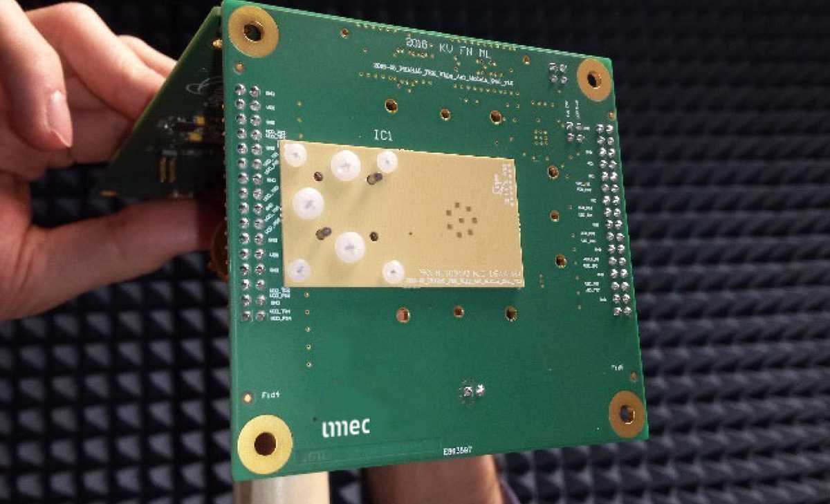
Figure 1: 60 GHz phased array wireless module.
Fabricated in TSMC 28nm CMOS technology, the 9.6mm2chip includes 8 transceiver front-ends to overcome signal losses at 60 GHz. The 8 paths are combined into one using a passive 8-way Wilkinson-based splitter/combiner to enable integration with another similar front-end chip (allowing range extension) or a baseband chip. This allows the chip to be useful for both mobile indoor applications such as 5G and WiGig as well as outdoor applications such as small-cell backhaul and fixed wireless access. A robust active phase shifter is also used in each front-end to enable steering the beam electronically without extensive calibration.
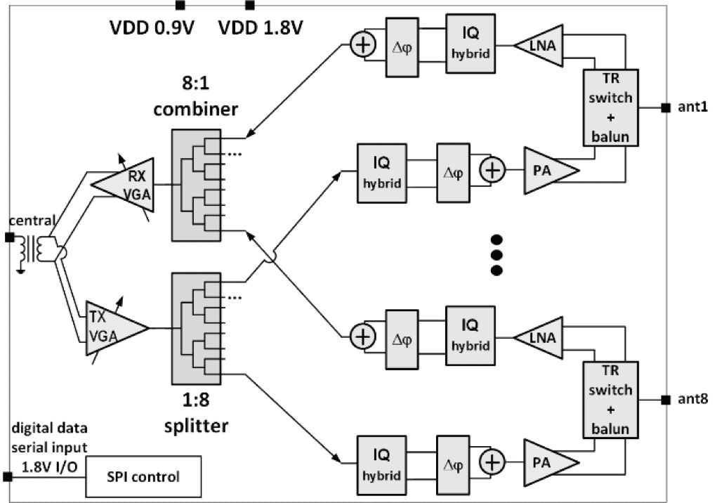
Figure 2: Block diagram of the 60 GHz phased array chip.
Efficient T/R switch and robust phase shifter
Instead of using a physical RF switch between the front-end and the antenna to switch between the TX and RX modes, only DC switches are used. The LNA input impedance is designed close to the PA output impedance so that they share the same balun. In this case, the last PA stage is a push-pull NMOS amplifier with Cgdcapacitive neutralization, while the first LNA stage uses an NMOS-based common-gate (CG) amplifier. The center tap of the balun is switched between VDDand ground. In TX mode, the center tap is connected to VDD. Therefore, the LNA input CG stage experiences VDD on both its source and drain nodes, switching it off and reducing the loading effect on the PA. In RX mode, the PA gate bias and the balun center tap are connected to ground. Similarly, the last-stage PA transistor terminals are all connected to ground, switching it off and reducing its loading effect on the LNA.
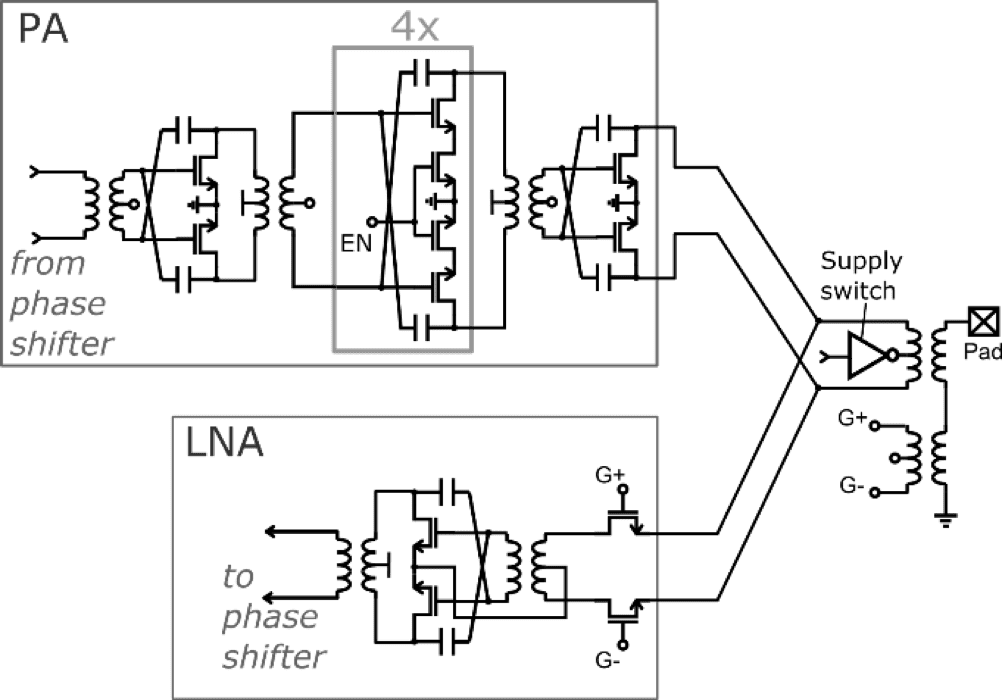
Figure 3: Front-end schematic including the PA and LNA.
The phase shifter is based on the vector summation of weighted in-phase (I) and quadrature-phase (Q) amplifiers using differential cascode configuration. The gain variation is made by splitting the cascode device into 5 binary bits including the sign bit. The 90º phase shift is implemented with a differential lumped equivalent of a Lange hybrid coupler that is placed between the common-source transistor of the cascode amplifier and its variable cascode array. An additional dummy cascode array is used to equalize the hybrid load impedance over the codes, minimizing the phase shifter amplitude and phase errors.
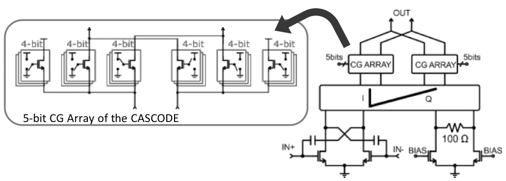
Figure 4: Phase shifter schematic including the variable cascode array.
Attractive performance
The chip achieves a TX output P1dB of 10dBm and an RX noise figure (NF) of 6.8dB (per path) and consumes 231mW in RX mode and 508mW in TX mode. The phase shifter achieves an amplitude error within ±0.35dB and a maximum phase step of 5º over the whole 360º phase difference. When integrated in a wireless module with a single patch antenna per path placed in a circular shape, less than 0.4dB peak-to-peak gain ripple is achieved over a 3dB scan angle of ±46º in both azimuth and elevation directions without phase shifter calibration. In this case, the gain and angle errors of a beam directed in a certain scan angle are a result of the average of the amplitude and phase errors of all phase shifters in the system.
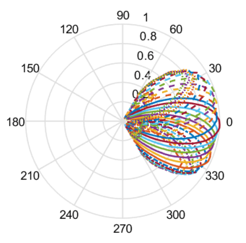
Figure 5: Radiation patterns of the module over the whole scanning range.
Wireless noise figure measurement and EINF
The RX noise figure is measured using the wireless module, where all RX path inputs can be excited simultaneously. When measured in a probed setup with only one RX path excited, the Wilkinson combiner becomes lossy, causing lower gain and higher noise figure that does not reflect the true operation of the chip. Instead, the wireless module faces an absorber and the output noise temperature is measured after being amplified with a waveguide amplifier. The module gain is measured in a another setup using a VNA and a horn antenna. This way, the module G/T, a parameter used to represent the noise performance of wireless systems, can be calculated. Normalizing the inverse of this parameter to the ambient temperature leads to the definition of EINF, which is a new parameter representing the effective isotropic equivalent noise figure and can be seen as the RX counterpart of the EIRP parameter for TX. Using this parameter, the RX noise figure can be extracted after the knowledge of the antenna gain (EINF = NF/Gr), and the link budget equation can be simplified to measurable parameters (SNRout= EIRP/EINF * FSPL / kT0B).
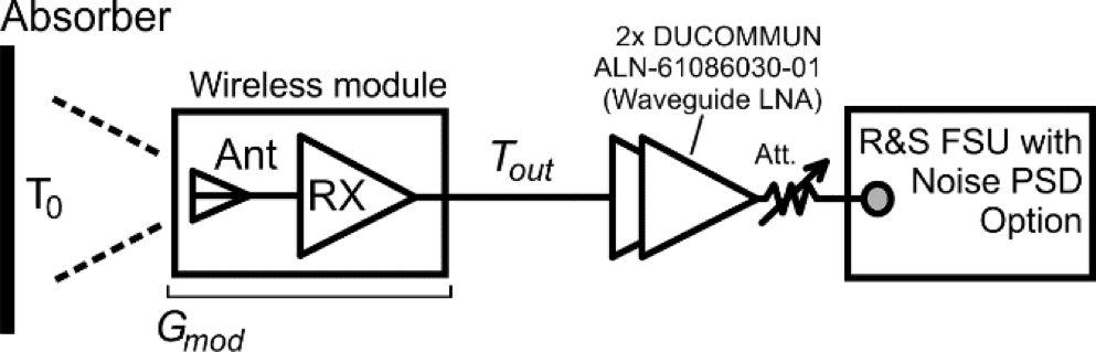
Figure 6: Wireless NF measurement setup.


