Silicon Micro-devices and MEMS Prototyping and Manufacturing
Design and development of manufacturing processes for MEMS, (active) micro-devices, sensors and detectors, embedded micro-systems and specialty components in Si CMOS pilot line.
From concept to prototype to manufacturable product
Imec is your strategic partner for translating a challenging device concept or prototype into a manufacturable product, tailored to your specific needs and specifications. Once the product is developed and fulfills specifications, we enable its low-volume manufacturing (up to 1000 wafers/year) by using imec’s fab. Moreover, in case high volume is needed, imec can transfer the process to a foundry in Asia – with which we have an established partnership. Alternatively, we can also transfer the process to your fab or to a foundry of your choice.
To develop your tailored component, our experienced engineering teams can rely on a wide technology portfolio and extended processing capabilities, including, for example, sensors, detectors, MEMS, 3D integration, Si and SiN photonics, wafer handling and packaging, and 90nm/130nm CMOS.
Imec is the only place where you can find an advanced 200mm/8-inch CMOS pilot line (which is also equipped for MEMS fabrication and 3D integration) that combines the process capabilities and quality of a foundry with the flexibility of a lab.
From concept to manufacturing
Imec’s dedicated development projects are bilateral, tailored to your specific needs. Our teams enable a product starting from either a concept or a prototype: we can develop a manufacturable process of a prototype you might already have, we can integrate on-chip your current product, or investigate how to tackle a specific application by using semiconductor technology.
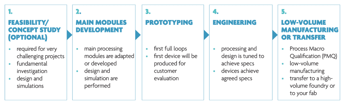
The product development can be divided into five main phases:
Integration and processing capabilities
For dedicated product development, imec uses its 200mm CMOS pilot line, which is also equipped for MEMS fabrication and 3D integration. It comprises:
Full CMOS compatible flow capabilities
- 193nm DUV ASML lithography available
Wafer handling and packaging
- Processing on Si, SOI, fused silica or glass
- Wafer thinning down to 20μm, grinding and CMP
- Wafer-to-wafer bonding: silicon or glass
- Chip-to-wafer bonding
- Wafer-level bonding of MEMS on CMOS substrates
- Custom post-processing on wafers from other foundries
Materials
- Broad variety of polymers for wafer-scale integration
- Low impedance, corrosion resistive electrode materials
- ALD with sub-nm thickness control, high-k dielectrics
- Electroplating of Cu, Sn, Ni
- Exotic materials introduction into CMOS environment and new material deposition development upon request
Special features
- Through-silicon wafer etch capability
- Bumping and through-silicon via integration
- Extensive in-line metrology and defect characterization, features down to 50nm
- State-of-the-art optical waveguide performance for visible light, NIR, IR
-
Integrated optical filter stacks

Chip to wafer bonding
Technology portfolio
At imec, you can find expertise in many different technology domains. This wide-ranging technology toolbox can be used to enable a chip for your application, or to tackle the challenges required to manufacture your unique device. Our technology portfolio includes:
- (Advanced) MEMS
- Si photonics
- SiN photonics:
- For processing SiN photonics components standalone or on top of a (foundry) imager
- Applications: sensors, spectroscopy, solid state lidar
- 3D integration
- Versatile platform to enable different type of device topologies
- Design and simulation
- Microfluidics
- Novel materials
- ...
Video
Pushing technology to the next level. The story behind the imec-ASML collaboration on EUV image sensors
MEMS & 3D integration
Imec has more than 20 years of experience in MEMS & 3D integration. Instead of focusing on standard and commercially-available MEMS processes, we can enable unique and challenging MEMS processes.
Imec has 2 MEMS platforms: SOI and SOI-bonded-on-CMOS. With the first platform, we can realize very large membrane devices such as microphones, pressure sensors, etc.The second platform bonds the CMOS wafers with the ASIC to the MEMS on SOI to realize monolithic integration between MEMS and ASIC.
Next to our processing expertise, we have a vast experience in MEMS design and modelling.
Advanced integration can be realized with our versatile, low-temperature 3D platform that features:
- Integrated passive device interposer
- TSV “middle”
- TSV “last”
- Direct low-temperature bonding (e.g. sensor on read-out IC)
- Microbumps chip assembly
- Wafer-level MEMS packing (high vacuum)
- Advanced active chip cooling (microfluidics)
Why companies choose imec
Imec combines the flexibility of a lab with an advanced CMOS processing tool set and non standard tools combined with the process capabilities and quality of a foundry.